A very belated Happy New Year to all. We are later than normal on this letter as we complete our open shuttle program with sponsor Google and partner SkyWater Technology (more on this later!).
We hope that you and your family, friends and colleagues are healthy and well in this time of COVID.
2020 was a year of continued change in hardware and semiconductors. Consolidation among leading IC companies continued apace, and companies like Apple, Amazon and Google continued to invest in their own internal IC design capabilities. Open source and open innovation in ICs picked up even more momentum – for some interesting perspectives here, please see the recap on 2020 by Gareth Halfacre blogging on behalf of the FOSSI Foundation.
This is all reinforces the urgent need to break with convention and open IC design to everyone. A world of billions, maybe trillions, of connected devices will require that IC design activity increase exponentially. Our role is to enable all of you to address this need by simplifying IC design and changing its economics to the point where software and hardware designers can create, at scale, the countless IC designs required for their IoT and Machine Learning applications.
How are we doing? Let’s review some of the milestones in 2020.
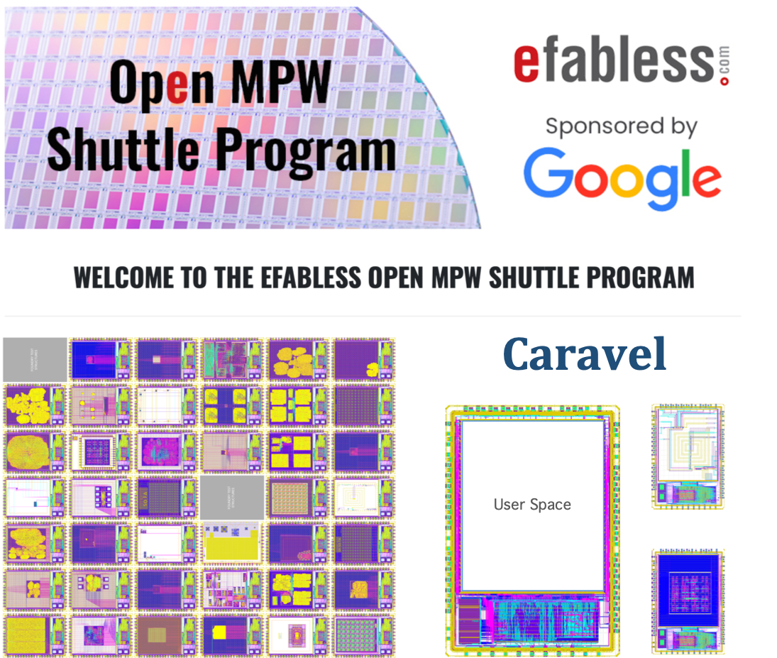
45 Designs in 30 Days
The Open MPW Shuttle Program demonstrates that removing the barriers of cost and access will enable a wealth of new and interesting IC designs. The Program is managed by Efabless, sponsored by Google and championed by Google’s Tim Ansell. SkyWater Technology played a key role by open sourcing its 130nm PDK, almost certainly an industry first. The rules were simple; create a fully open source design and Google would pay for your prototypes.
The results? In 30 days, the forty available slots were oversubscribed with submissions from a global community of professionals and academics, ranging from IBM to a college freshman. The majority were embedded software developers and hardware designers – not IC experts. And that is the point, opening IC design to the IC users for more, better and more relevant solutions!
There were SoC’s; processors, embedded FPGA’s (including two from QuickLogic) and analog, digital and mixed signal IPs. Examples included a crypto-currency miner, a satellite transceiver and a robotic application processing core.
In addition to managing the project, Efabless delivered a complete chip development flow, called OpenLane.io, incorporating the DARPA-funded no-human-in-the-loop OpenRoad project, and validated it with the open source striVe family of IC designs.
Efabless also created and released into the open source Caravel, a fully implemented ASIC design template that allows users to easily integrate their digital or analog designs inside a carrier test chip with a management RISC-V processor, SRAM and user-controllable IO pad-frame. Caravel simplifies community design development and validation by allowing the designer to focus entirely on their specific design idea and not worrying about other necessary functionality to bring an idea to silicon.
The future? More shuttles, more designers and more designs. With the barriers removed, software and hardware developers will create the silicon that makes their products the best they can be. Silicon like software!
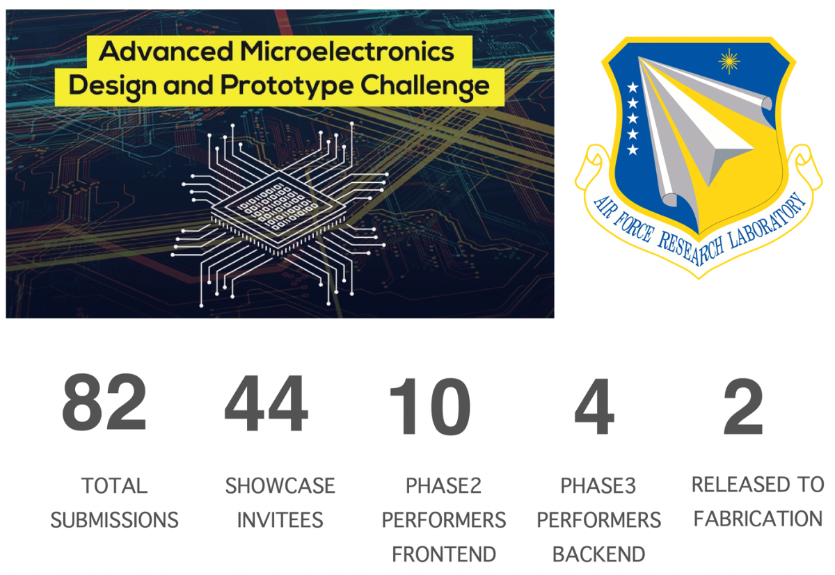
And 82 SoC Design Proposals
in < 2 months
Speaking of the unlocking untapped design potential. The Open MPW Shuttle Project is similar in many ways to AFRL‘s (Air Force Research Laboratory) design challenge for 14nm IC designs that enable autonomous applications. In that case, 82 unique IC designs were submitted in 45 days – 80 percent from small enterprises and academics. Here the designs were proprietary, but the entrants had to agree to publish their IC designs, the intended applications and other key information in order to enter the challenge. If you were chosen, the cost of IP, EDA and foundry would be covered. Efabless served as a subject matter expert and kudo’s to AFRL (led by Len Orlando), AFWERX and Centauri (a KBR company) for their creativity and tireless efforts in this groundbreaking initiative.
The project which commenced in late 2018, came to its successful conclusion in 2020, further illustrating that when barriers are reduced more designs can get to prototype – and in numbers that were never imagined!

NEC: Secure IC’s thru Open Reference ICs
NEC and its NEC Research Labs team under Managing Director Tsvi Lev demonstrated how open source delivers secure ICs through maximum transparency. NEC utilized the Efabless design network to customize the Raven open source microcontroller reference design, offered in our marketplace. NEC presented their findings along with Efabless at the ChipEX2020 conference in September 2020.
Collaborations to Open IC Design
Efabless open platform makes silicon design inexpensive and simple using pre-engineered templates and a web-driven configurator. We are collaborating with imec, to combine our low cast, fast IC development with their world class supply chain solution – fab, assembly and test. Silicon Catalyst, the leading incubator for ICs, added Efabless as an in-kind partner to provide a fast, affordable and easy path to proof of concept ICs for its portfolio companies.
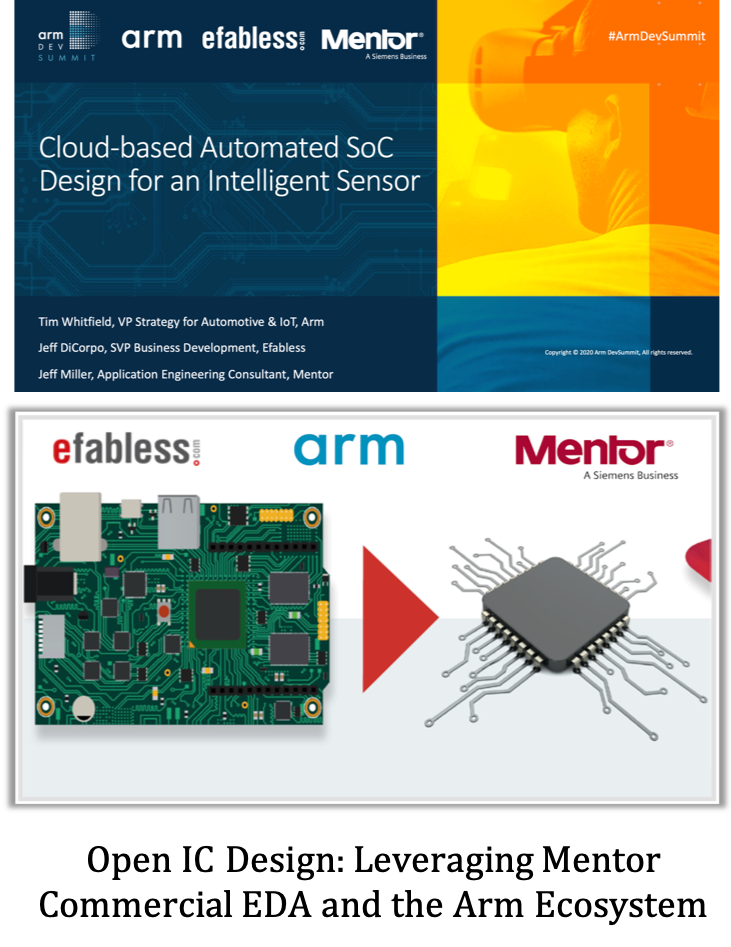
Mentor Tools on Efabless Platform
At Arm’s DevSummit 2020, Efabless co-presented with Arm and Mentor Graphics on delivering custom silicon for sensor applications using the Tanner design flow, Arm-based templates, and foundry (XFAB) IP, executed on the Efabless platform.
Customers & Partners
![[object Object]](https://umsousercontent.com/lib_CUsguFEVafmoKCKW/ns6hm1s6vu8ctynd.png?w=334)