![[object Object]](https://umsousercontent.com/lib_CUsguFEVafmoKCKW/ns6hm1s6vu8ctynd.png?w=334)
Your Own Hydra
Part 1 of this article showed how to clone an open-source project from the Efabless IP marketplace and view it in your own workspace on the Open Galaxy platform. But the purpose of cloning a project is so that you can not only view the existing design, but also so that you can use the design as a starting point for your own project. This part of the article, in addition to being a how-to about the process of creating a chip using the tools available on the Efabless platform, also highlights the relative ease and simplicity of getting a complete chip designed, verified, and ready for tape-out using the Chiplicity methodology.
The Hydra chip (hydra_v2p0) was designed as an open platform with a general-purpose padframe that can accomodate inputs and outputs from any IP blocks placed in the chip core. Some of the IP blocks are open-source, and many are closed-source, meaning that you cannot view the details of the project. The closed-source entries cannot be cloned, so you cannot run characterization tests on each block individually. But you can use the “Try This IP” option for any item in the Efabless IP Marketplace that allows it, which will provide you with a read-only view of the IP block that is sufficient for placing in a chip design, and will allow you to characterize and verify the project as a whole without specific access to the read-only IP blocks.
The SPI controller used on the Hydra v2p0 chip is specific to the IP blocks on it. To make your own test chip, you will want something more general-purpose for communicating with and configuring the IP blocks that you choose for it. In the IP catalog is a general-purpose SPI controller called “ef16_spi_controller” that has 12 output registers of 8 bits each and 4 input registers of 8 bits each (see the documentation in the IP catalog). Although replacing the existing IP controller with the general-purpose one requires some amount of rewiring on the top level, all the tools are in place to wire up the top level and validate all the connections.
In this part of the article, I outline a (relatively) simple chip design, similar to hydra_v2p0 and based on the same padframe, but with different internal IP blocks and the general-purpose controller. To keep it simple, this example chip will retain the same padframe (and therefore the same I/O) as the hydra chip. The IP blocks on the Hydra will be replaced with IP from the X-Fab analog IP set.
Getting the EF16_SPI_CONTROLLER IP
As in Part 1, you will want to navigate to the Efabless IP Marketplace and display the Community IP results in the catalog. From there, find the IP block “EF16_SPI_CONTROLLER”.
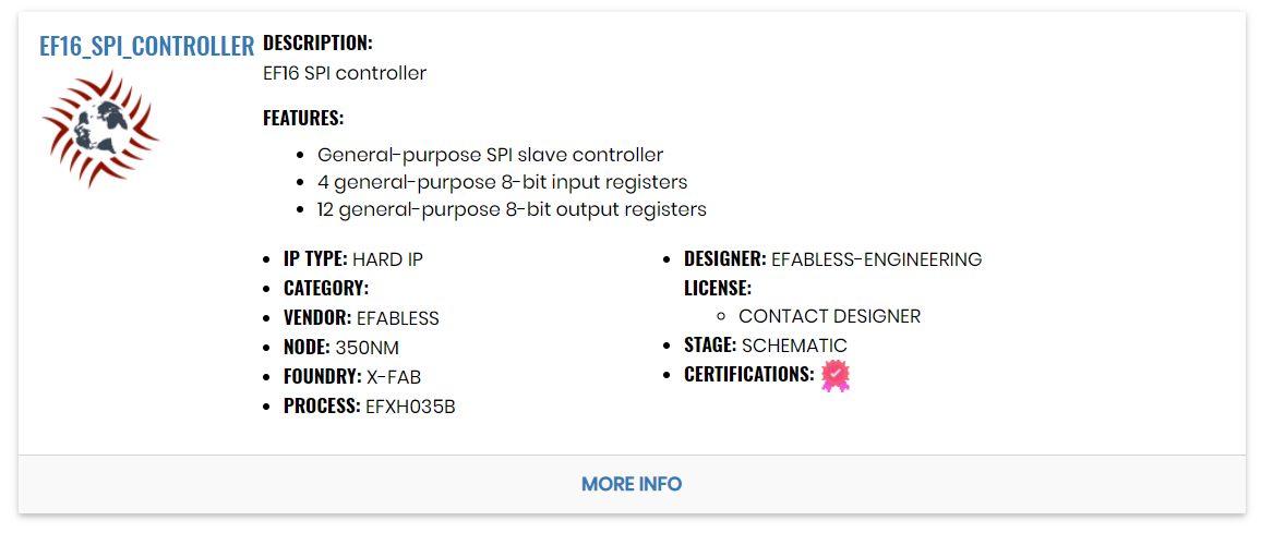
Click on either the IP name or the “More Info” button to access the detailed view of the IP.
On that page, unlike the page for the Hydra chip project, you have the choice of “Try Hard IP” instead of “Clone Hard IP”. The difference between “Try” and “Clone” is that a “cloned” project becomes a project of your own in Open Galaxy, and is completely editable, and may be changed by you in any way. With a cloned project, you get schematic and layout views, and can modify circuit components and change the layout. By contrast, an IP block that you “Try” does not become a project in your Open Galaxy workspace, but can be pulled into another project by accessing the symbol of the IP in the schematic editor, and an abstract view of the layout in the layout editor. If the IP blocks are marked as “efabless certified” in the IP marketplace, then you can be assured that they have been fully characterized, and the layouts are DRC clean, and the schematic and layout are guaranteed matching.
The EF16 SPI controller is “read-only” IP not specifically because it is closed-source, but because it is not easily editable since it has been built with a digital synthesis flow. For the purpose of having a digital communication channel to your own chip, it is convenient (for this article) to have this general-purpose interface instead of the much more complicated process of starting from a Verilog source file and synthesizing and verifying a custom digital block.
Click on the “Try Hard IP” button now. You will get the same notification that the IP is available in your MyLib space as you did for the Hydra project. If you go to the MyLib space, you will see that the EF16 SPI controller appears in the “Marketplace Items” list rather than the “Private Items” list, indicating that it is not a cloned project, but rather read-only IP that is being made accessible to your projects in Open Galaxy.
Getting Other Read-only IP Blocks
Now we will select some other IP to make our own chip version. Go back to the IP Marketplace, and this time select “Foundry” as the IP Provider.

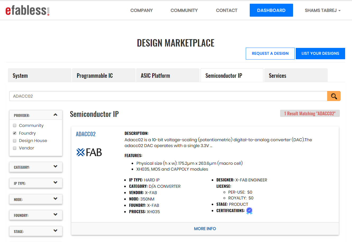
Select “ADACC02” (type “DAC” as a search term in the search bar if you have trouble finding it in the list),
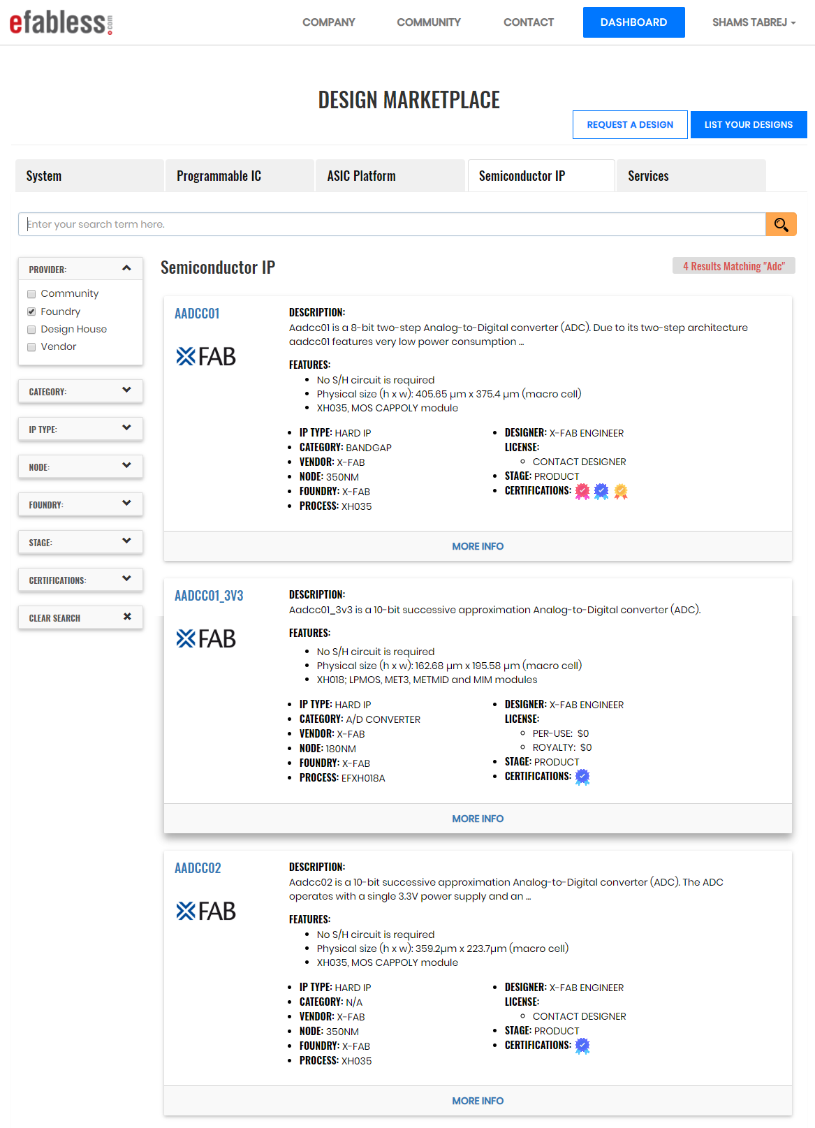
Navigate to more info and then click on “Try Hard IP”, just like you did for the EF16 SPI controller.
Do the same for “ACMPC01” (use search term “comparator”) and “ARCOC01” (use search term “oscillator”). For each of these IP blocks, click “Try Hard IP”; when you’re done, you can find them in Library listing.
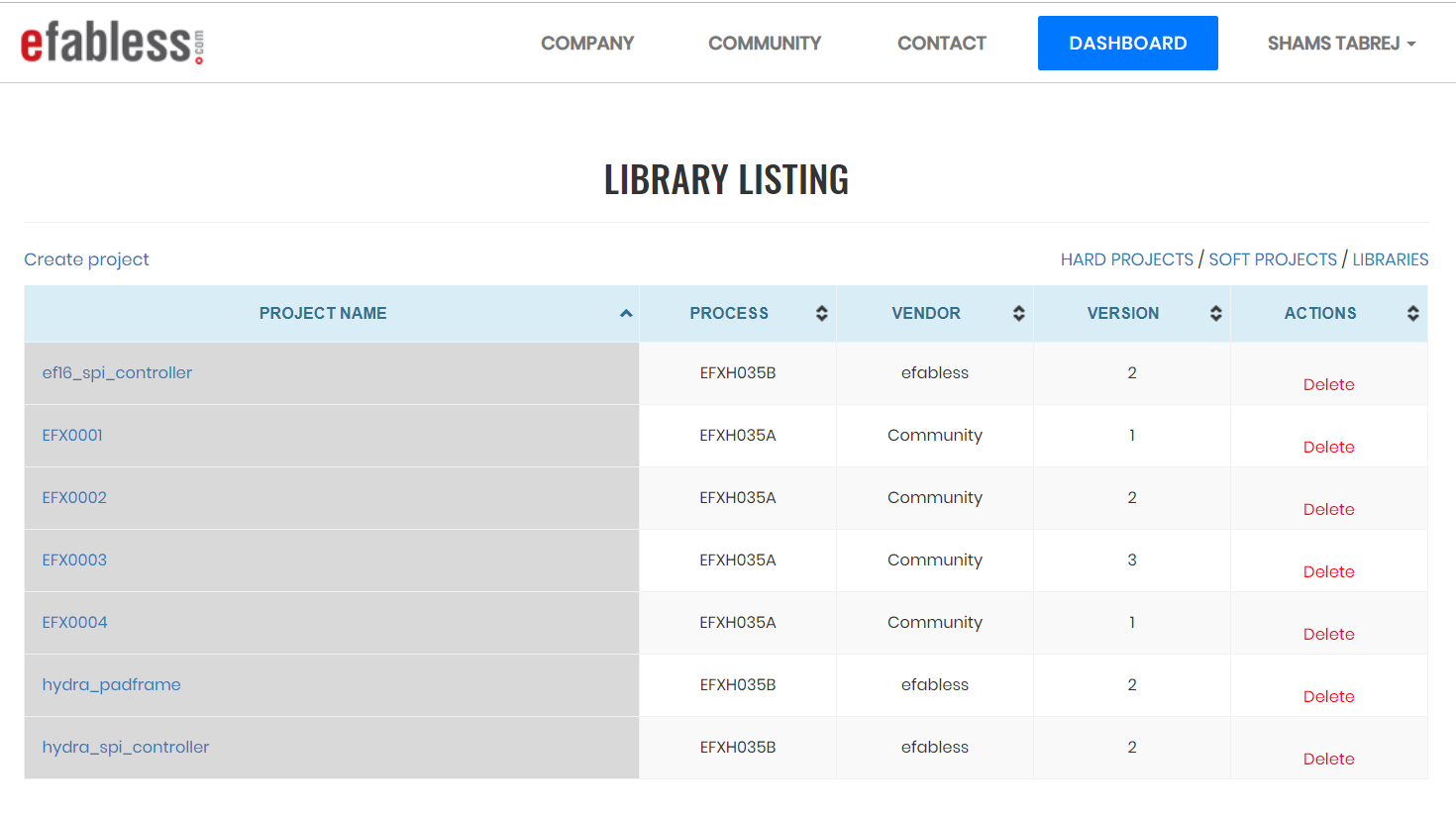
Then go to Open Galaxy and complete the synchronizaton process as before.
Note that the IP blocks “ACMPC01”, “ARCOC01”, and “ADACC02” are listed in the IP catalog but are really part of the foundry PDK. As such, they do not need to synchronize to your Open Galaxy work space, and if you have already synchronized the SPI controller, then you may see the message “Not synchronized (0)”, suggesting that there are no items to sync. Go ahead and click on “Okay”.
Now you’re ready to build out your own chip.
Editing the Schematic
This article will assume a basic working knowledge of schematic entry using Electric and layout entry using Magic. If not, there are tutorials and documents in the efabless Knowledgebase to help you out.
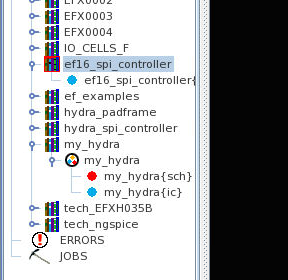
Start Electric using the project manager’s “Edit Schematic” button, which starts Electric. If you followed the first part of the article, then you found and expanded the my_hydra library in the Components window, and the schematic or symbol view should be remembered and automatically come up in the window. Make sure you are editing the schematic view.
Clean out the parts of the original hydra chip that won’t be used here. Somewhat arbitrarily, for the purpose of this article, keep the ADC, and the POR (which is needed to reset the SPI controller properly), but delete all five of the bandgap circuits. Remove the original SPI controller.
Because the EF16 SPI controller was downloaded after the “my_hydra” project was already made, it does not automatically show up in the Components sidebar tab. However, it has been made accessible to your project by MyLib. Go to the “File” menu button, and select “Open” from the drop-down menu.
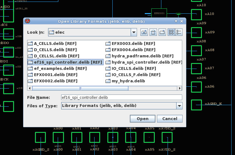
The library “ef16_spi_controller.delib” should be one of the items listed, and you can select it, and it will then appear in the Components window.
From the Components window, you can select it with a mouse grab and drag it into the schematic editor window, and place it in the schematic.
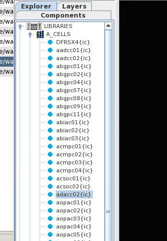
The new blocks from the X-Fab IP, “adacc02”, “acmpc01”, and “arcoc01” are part of the PDK, as mentioned above, and can be found in the library “A_CELLS” which is one of the libraries that is always shown in the Components window for this PDK. If you expand the A_CELLS entry, you can find these three cells and drag them onto the schematic.
There is one additional item that will become clear when wiring: The “acmpc01” has an input “VBN”. What should be done with it? Well, if you go to the IP catalog and select “acmpc01” again, one of the options to select is “View Datasheet”. Click on this and you get a PDF file describing the comparator. In the description is the following text:
Description of X-Fab comparator IP block.
So it is clear that an additional IP block, the “abiasc03”, is recommended. Since this block is also part of the X-Fab A_CELLS library, you can find it in the efabless IP catalog, select “Try Hard IP”, and sync it to MyLib; or, since it is a cell in the foundry PDK, you can bypass MyLib and just select it from the A_CELLS list in the schematic editor. Either way, it goes into the schematic, next to the comparator.
Once all the cells are on the schematic, it is just a matter of wiring them up. Select appropriate inputs and outputs of the SPI controller to connect to these blocks. This is the view prior to any wiring:
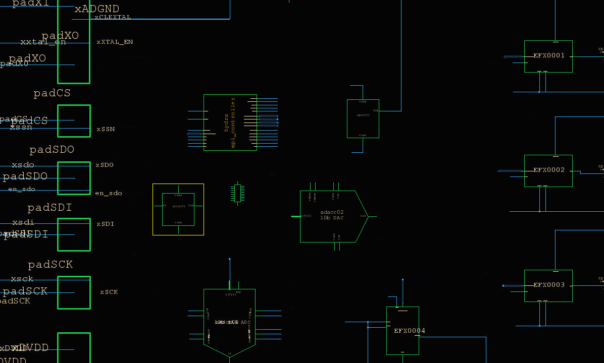
“Select appropriate inputs and outputs” is a significant task; keeping track of how all the IP blocks connect to the IO and to the SPI and where they appear in the SPI register set is mainly a bookkeeping task, but very important for quickly referencing these connections for layout and for writing and analyzing functional simulations. Here is a list of possible connections. For the chip pins, two of the bandgap IPs used two pins each, and since we need four additional pins for the new IP (DAC high and low reference inputs, and the op-amp positive and negative inputs) we just connect those to the new IP blocks. The digital registers are assigned arbitrarily.
- xA04 = DAC VREF low
- xA05 = DAC VREF high
- xA06 = RC Oscillator output
- xA07 = RC Oscillator power supply
- xA08 = DAC output
- xA09 = DAC power supply
- xA10 = Comparator output
- xA11 = Comparator and bias power supply
- xA15 = Comparator positive input
- xA16 = Comparator negative input
These are the names of the top-level nets connected to the digital (SPI) buses:
- inreg4 = D[7:0]
- inreg5 = D[15:8]
- outreg8 = A[7:0]
- outreg9 = A[15:8]
- outregA = B[7:0]
And here is where the various IP block control inputs and digital outputs connect to those named buses:
- D[9:0] = ADC data output
- D[15] = ADC end-of-conversion (EOC)
- A[9:0] = DAC data input
- B[5] = ADC convert (start)
- B[4] = ADC enable (rstb)
- B[3] = RC Oscillator enable
- B[2] = Crystal oscillator enable
- B[1] = Comparator bias enable
- B[0] = Comparator enable
The main point of the exercise is to ensure that all blocks can be properly controlled from the SPI, and that all blocks whose output is to be measured have access to pads on the padframe. Keep the resistors that were used on the hydra_v2p0 for ESD protection of the internal IP blocks between the IP block outputs and the pads, since the pads only partially protect against ESD events.
This is a completed schematic after wiring up the subcell blocks as described above:
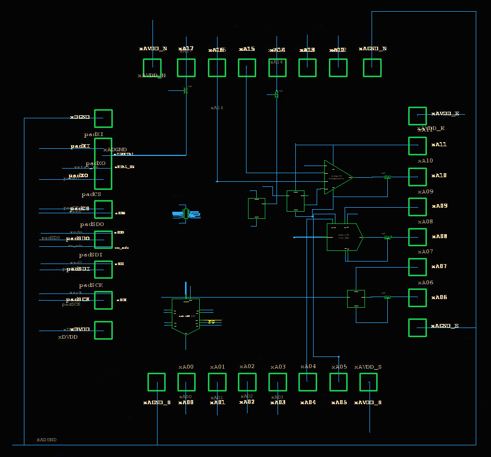
My Hydra schematic.
After creating the schematic, be sure to do “Save Library” to save the result.
Editing the Layout (and Verifying DRC)
One way to build a layout and make sure you have all the components is to start with an existing layout and modify it to suit your needs. The other way is to start with no layout and click on “Edit Layout” in the project manager, which will then create a new layout for you with all the components. However, it will make no attempt to arrange the cells or wire them together, and will place all components in a row. For this “my_hydra” project, either method probably involves the same amount of work. This article will use the method of starting with the existing project and modifying it.
From the layout editor, clean out the existing IP by selecting each one in turn (using Control-i to select the cell) and deleting it (use the “d” key to delete). Like in the schematic editor, remove the existing SPI controller and the five bandgap cells. Remove the wiring surrounding these cells and leave plenty of room around the SPI controller (the EF16 SPI controller is significantly larger than the original on Hydra v2p0).
To see the library cells that are available to the layout editor, select menu item “Options” and then “Library Manager”. You can open the various libraries you need; the X-Fab analog cells are in library “A_CELLS”, and each IP block is in its own library (you’ll need to grab “ef16_spi_controller”), and then place each one by positioning the white “cursor box” at the lower left corner of where you want the cell to go, and click on the “Place” button in the library manager. However, you may find it easier to get the cells using the command line in the magic console window. You can import any of these cells using the command “getcell”. So place the cursor box in the position you want each of the new IP blocks, in turn, and do:
getcell ef16_spi_controller
getcell acmpc01
getcell adacc02
getcell arcoc01
getcell abiac03
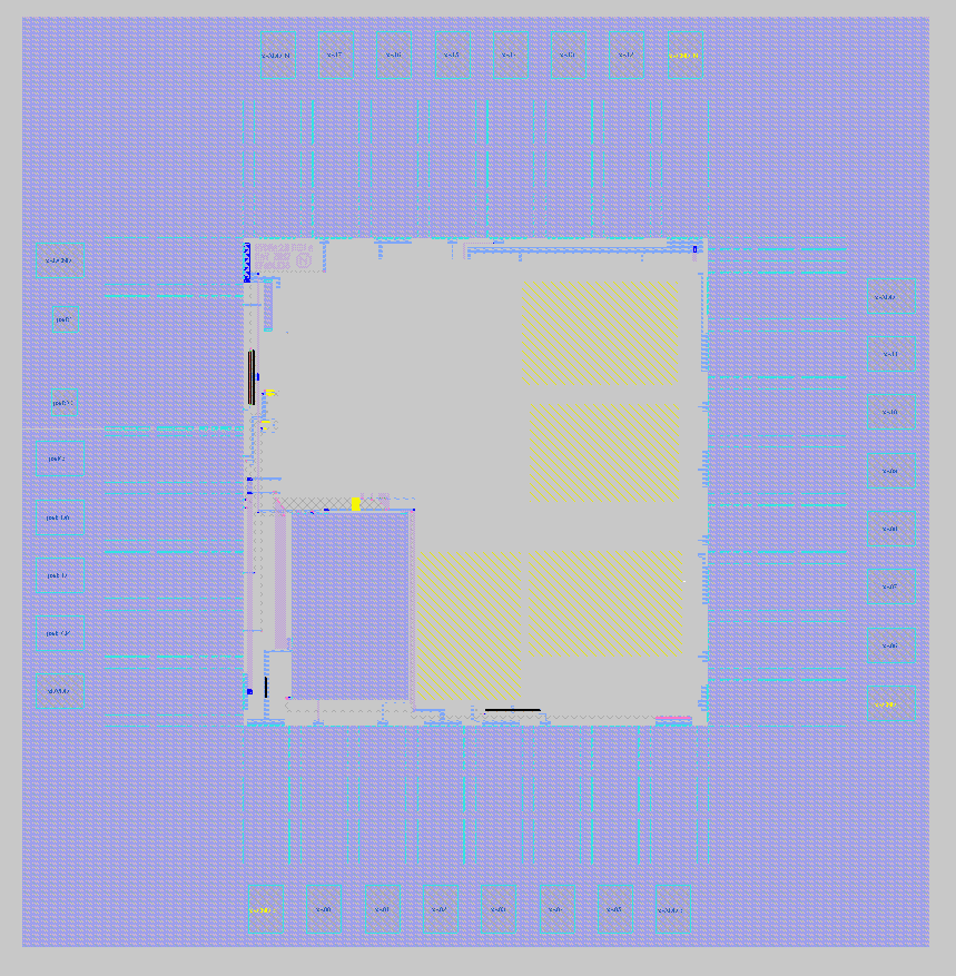
From this point, wiring the chip is basically like any other layout on the platform. The layers available to you are the metal layers and the vias for connecting them, and some additional layers for substrate contacts which you should use to make sure that the substrate is well-connected, especially close to the IP blocks. The antenna cells used on Hydra can be re-used on all gate inputs that may be sensitive to ESD events. Each IP block only differs from regular devices in the PDK in that only metal layers are shown. All pins that need to be connected are marked, and should match pins of the same name in the schematic view. Below shows a view of the my_hydra chip after initial routing of analog and digital signals.
Pre-LVS completed top-level layout.
Use the labeling feature (menu item Edit->Text for a text helper dialog window) to name nets at the endpoints so that it is easier to figure out where to route. Routes can be made with the wiring tool, or with the “fill” and “corner” commands. See the various online documents for help with using the layout tool.
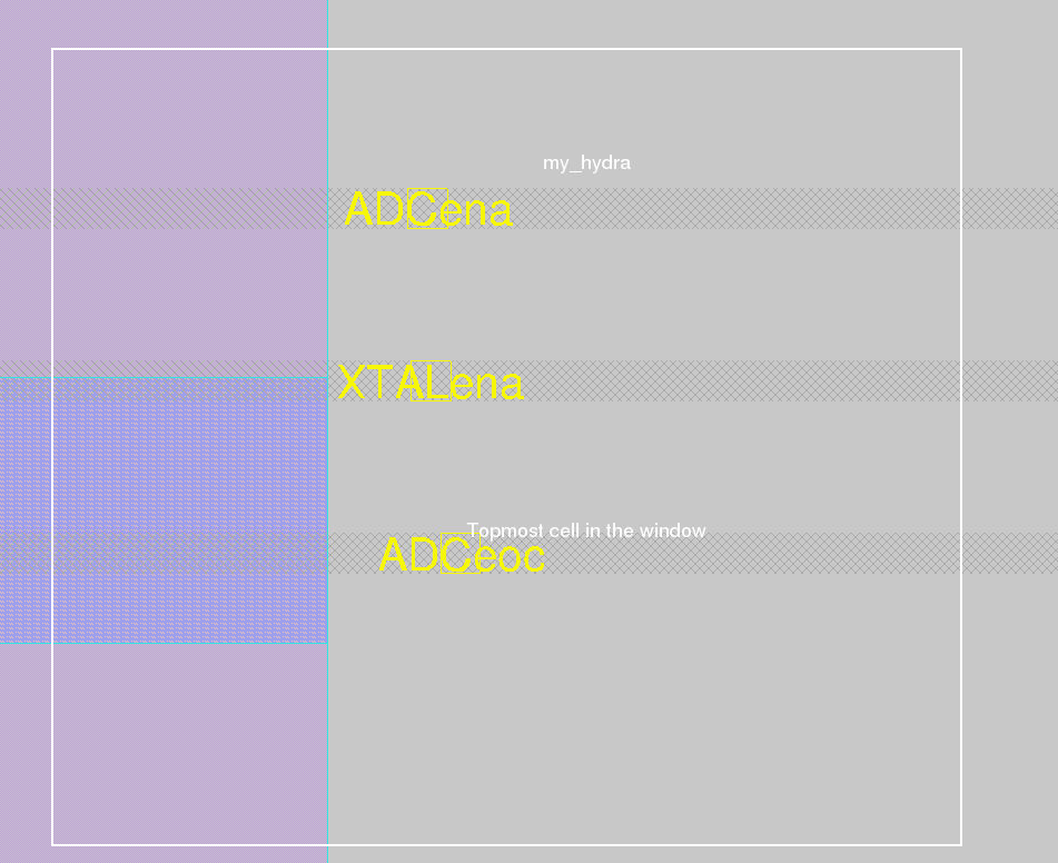
Labeling nets to help with wiring.
The layout view below shows the resistors that are placed between unprotected IP block outputs and the padframe analog I/O cells. The aspect ratio of the device has been changed using the device properties dialog window (select the cell with Control-I and type the “q” key for the properties window). Otherwise, the device is unchanged in effective value. A substrate contact has been placed next to the device to help keep the substrate at ground close to the (grounded) nwell of the resistor, to avoid latchup (forward biasing of the well).
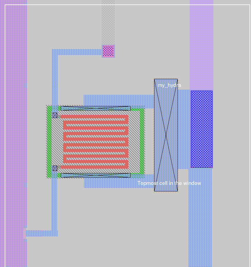
Resistor placed between unprotected IP block outputs and the analog I/O pads.
Finally, all digital inputs and any other signals that comprise a small area of MOSFET gates connected to a long wire, with no p+ or n+ diffusion connected close to the MOSFET gates, can be an antenna rule violation: the metal wire acts as an antenna to collect charge, potentially generating enough static charge to destroy the connected MOSFETs. The antenna cell from the hydra_v2p0 layout was kept and was copied to each such potential antenna rule violation, connecting the signal wire to the n-diffusion and connecting ground to the substrate diffusion, as shown.
Antenna cells from hydra_v2p0 used to avoid antenna rule violations.
Verifying LVS
Because everything inside each IP block has been abstracted, LVS becomes easier than otherwise because the LVS report will only show the IP blocks and their pins. Any wiring error that might accidentally short something inside an IP block will collide with the metal obstruction layers in the IP block’s abstract view, and so will show up as a DRC error. So make sure that you have resolved all DRC errors prior to running LVS. The design must be both DRC and LVS clean, to be validated and given an Efabless certification. For LVS, click on the “Run LVS” button in the project manager, and in the LVS tool, click on “Run”. As long as you have saved a valid layout and a valid schematic, the netlists should be generated automatically. A typical LVS result is shown below.
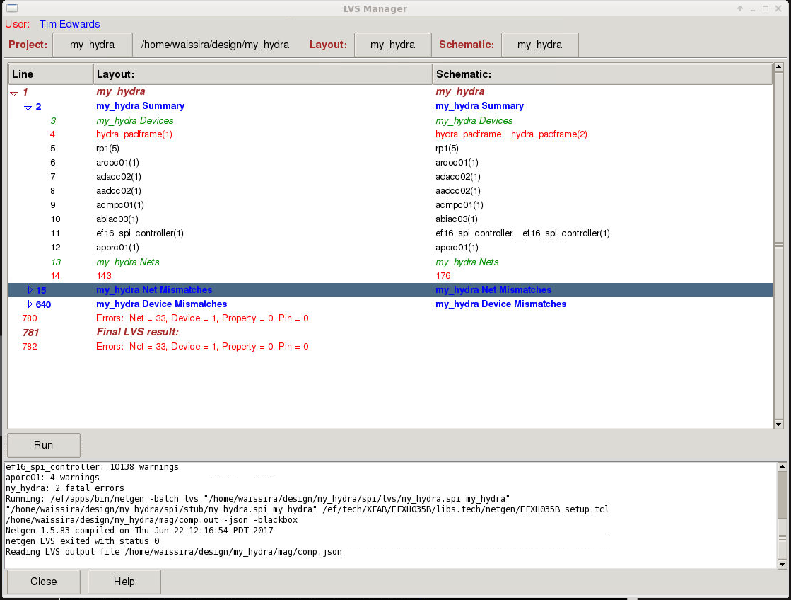
For help with identifying and correcting LVS issues, see the knowledgebase articles on the subject. Errors in the number of devices is the first thing to solve. In the LVS result above, the schematic has managed to end up with two copies of the padframe, which is an error that needs to be fixed in the schematic before proceeding with debugging any wiring errors. In the layout and schematic shown here, the errors ended up being, in addition to the overlaid padframe symbol in the schematic; a reversed bus in the schematic, failure to connect the ground nets in the layout, and failure to route a handful of signals in the layout, all of which were relatively easy to determine from the LVS output and fix. Below is the final LVS report, showing an LVS clean result.
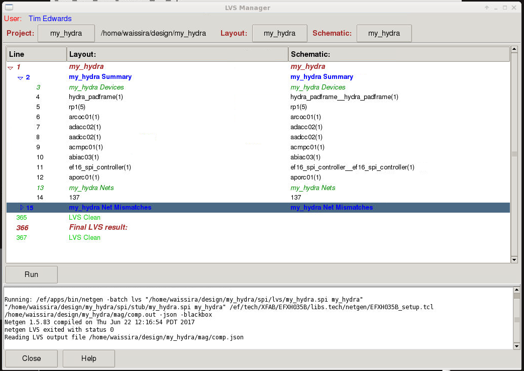
my_hydra LVS clean report.
Verification by Simulation
The next big step is to verify the chip functionally using full-chip simulation. This is be covered in Part 4 of this article.
Fabrication
The last and final step is to get your chip fabricated. Because foundry data is proprietary, GDS data is not viewable on the system to Open Galaxy users. However, from the various layout views, the data exists on the system for the GDS output to be generated, and Efabless can submit the layout for fabrication.
Although at this point in the process I have not verified the functionality of the chip, I have a complete DRC and LVS clean layout that is (pending simulation results) ready for tape-out, and it was all done end-to-end from the Efabless platform using the open-source tools provided on the platform. Making the chip was essentially a one-day project, with the strong caveat that this is a demonstration chip, and the components on it are largely independent of one another and were chosen more or less at random from the available IP blocks. However, that said, obtaining all the IP blocks needed for the project took about 30 minutes or so. Creating the schematic took another 2 hours or so. Creating the layout took about 4 hours. Running LVS and fixing errors required approximately an additional hour. Although I spread those tasks over several days, the total time involved was less than one workday for one person. I have been building chips for over 25 years, large and small, and this was by far the fastest time I have ever experienced for getting a design ready for fabrication, even if I consider only the steps involved (schematic, layout, and DRC and LVS verification). I hope that I have been able to demonstrate here that Chiplicity is the right way to design chips!