![[object Object]](https://umsousercontent.com/lib_CUsguFEVafmoKCKW/ns6hm1s6vu8ctynd.png?w=334)
Simulation with Chiplicity
The first part of this Knowledgebase series alluded to running characterization on a full chip. Full-chip simulation is not a trivial task, and in general is not possible using SPICE to simulate everything at the transistor level. Since SPICE generally has difficulty with fast-changing signals, digital circuits in particular will slow down a simulation dramatically if simulated at the transistor level, as will switched-capacitor circuits.
Two recent developments in ngspice come to the rescue of full-chip simulation, making it realistically feasible for the first time. The underlying method that made these developments possible is XSPICE, which is an event-driven cosimulation engine integrated into SPICE. XSPICE has been around for many years, and has been part of SPICE distributions for many years, but (possibly due to lack of good documentation) it has been largely overlooked. This is unfortunate as having an event-driven cosimulation environment in SPICE is exactly what is needed for full-chip simulations.
One of the drawbacks of XSPICE is the need to write C code for new simulation primitives, and the set of primitives traditionally included with XSPICE was very basic. For example, the digital gate primitives contained the usual set of gates like AND, OR, INVERT, XOR, and so forth, but this is not enough to represent any full-featured digital standard cell set. Recent development versions of ngspice have a new primitive (written by yours truly) called “d_lut” that is able to represent any digital gate with N inputs and one output, and a primitive called “d_genlut” that is able to represent any digital gate with N inputs and M outputs. Those primitives, along with the original flip-flop and latch primitives, can represent entire standard cell sets. A script can make a direct conversion between a SPICE netlist of digital cells and the equivalent XSPICE circuit, and suddenly huge digital subsystems can be simulated quickly and efficiently without over-tasking SPICE.
The second improvement is another XSPICE primitive written by Glen Ramalho that sets up a communication pipe between SPICE and iverilog (icarus verilog), running independently as separate processes. SPICE tracks what the iverilog process is doing by declaring an XSPICE primitive called “d_hdl”, while iverilog tracks what the SPICE process is doing by defining and declaring a function called $d_hdl_sync(). Iverilog starts SPICE from inside this function. The communication pipe limits the ability of the two sides to synchronize with each other, but the system works, and allows testbenches to written in verilog. With functions and tasks and such, this is a powerful way to drive a system’s inputs and collect outputs, and because it is event-driven, it is very fast to simulate.
The efabless cosimulation environment makes use of both of these methods for full-chip simulation. Since the verilog-driven cosimulation method runs SPICE from inside verilog, that implies that only one verilog process is running, so only one circuit in the system can be defined in verilog. So this method is used to define the testbench stimulus (or at least the digital part of it; it remains easier to drive the analog stimulus from the SPICE netlist as long as the analog components are doing simple things like pulsing continuously or ramping up or somesuch). The stimulus directly drives (and receives input from) the chip pads, so the netlist remains exactly as it came from extraction (other than to substitute different views for some subcircuits; see below). Everything inside the chip is either represented in the netlist at the transistor level, or at a functional level using XSPICE (for digital, as described above, but also for analog circuits using some of the more obscure analog XSPICE primitives, such as gain and multiplier blocks, and other useful and powerful primitives), or other simplified SPICE representations using nonlinear sources and embedded functions, which simulate more efficiently than the equivalent circuit built out of real (i.e., manufacturable) device models.
Note that the goal of full-chip simulation and characterization is to test the functionality of the whole system. Each individual component is assumed to have been already fully characterized, as it comes from the Efabless IP catalog and is certified by Efabless before it may appear there. Of course it is best to be able to get as realistic a simulation as possible. So the goal of full-chip characterization is to enable the full analog view of each component as it is put under test for functional verification. In extreme cases, complex and difficult-to-simulate blocks like an entire ADC may require always simulating as a simplified functional view.
Simulating “my_hydra”
The discussion above sets the context for the full-chip characterization of the example project “hydra_v2p0” which, in part 1, was cloned into a local project on the Open Galaxy platform called “my_hydra”. The full-chip simulation is set up in the same CACE (Circuit Automatic Characterization Engine) system used for the Efabless challenges. Like those challenges, the characterization comprises two parts: The datasheet, or spec sheet, which describes the conditions under which each test will be made and the limits for acceptable behavior; and the testbench, which is a netlist describing the test setup and including the device under test. The full-chip simulation includes a third component, which is an additional testbench file in verilog format describing the handling of digital signals into and out of the chip. All three files (datasheet, testbench SPICE netlist, and testbench verilog) need to be carefully coordinated.
The project manager in Open Galaxy should look like the image below after following the steps of part 1 of this article, and assuming the cloned project was named “my_hydra”.
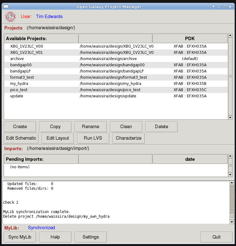
Project Manager after cloning the hydra_v2p0 design into project “my_hydra”.
To simulate the my_hydra project using the CACE tool, click on the “Characterize” button. The characterization tool will then launch, showing all of the testbenches that have been prepared for functionally testing the hydra project.
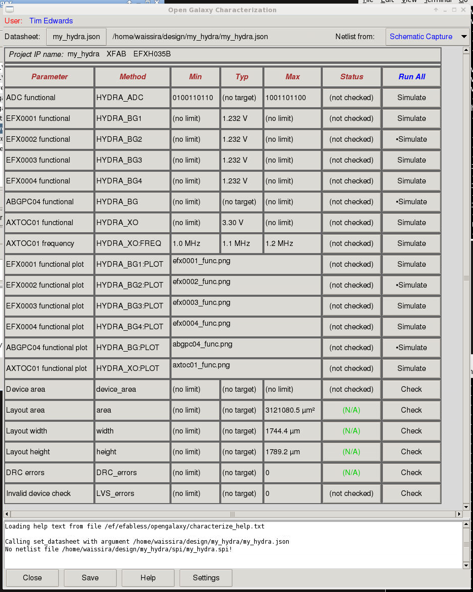
Characterization tool view of the my_hydra project before characterization.
Simple Physical Characterization
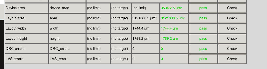
Before getting into the problem of running full-chip simulations, there are a few simple characterization checks that can be run on the “my_hydra” chip. These include the chip area, width, and height, and a device check to ensure that all devices are valid for the foundry process (check done on the schematic view), and DRC and LVS checks (done on the layout view). By default, the source netlist is set to be the netlist captured from the schematic view, and tests (where applicable) are run on this netlist. The source netlist selected is indicated in the top right-hand corner of the characterization tool window.
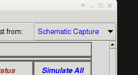
Characterization tool source selection button
The bottom of the characterization tool view shows all of the physical tests. Because the schematic captured netlist has been selected, the physical dimensions are not available (yet; see below). The schematic extracted results includes a “device check”. For IP blocks made from low-level circuit components such as transistors and capacitors, this test shows whether the devices in the schematic are all available as layout views in the PDK. For projects like the hydra, which are made from lower-level IP blocks, this test checks that the IP blocks exist and are readable, since they are located outside of the immediate project. For this check, click on the individual “Check” button next on the “Invalid device check” row. Do not click on “Simulate All” at this time, as it will run all the functional tests, which take much longer than physical parameter checks, and are explained below. The result of the device check should indicate a “pass”. The label “pass” is on a button that you can click to see the full text of the device check results, as shown here:
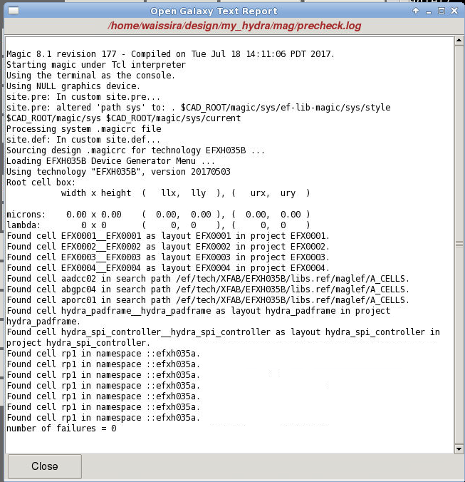
Result page of the device check for the my_hydra project.
You can also run the “device area” check from the physical parameters while the schematic netlist is selected. Note, however, that this simply sums the areas of individual IPs. Because one of the individual IPs in the full chip is a padframe, the device area check double-counts the core area of the chip, which must be taken into account when interpreting this value.
If you change the netlist source to “Layout extracted”, then these tests will measure the chip physical dimensions from the layout. Be sure to save the characterization results before changing views (simply click the “Save” button at the bottom), as otherwise they will be lost and will have to be repeated if you want to view them again.
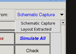
Characterization tool source selection menu.
Again, click on the “Check” button on individual tests for the chip area, width, and height, since doing a full run of all functional tests is explained in detail below. After running the physical verification on the layout netlist, save the results again with the “Save” button, and be sure to return the netlist view to “Schematic Capture” for functional verification.
Full-chip Simulations
As noted above, functional testing is currently only supported for the “Schematic Capture” netlist source (as determined by the button in the top right corner). The functional simulations are actually an amalgam of layout-extracted views of each IP block and a schematic-extracted top level. IP blocks are read-only, protecting the device-level circuit from being viewed by the end user, but the layout-extracted netlists are visible to the simulator. Each testbench netlist can specify whether or not an IP block should be substituted with a functional view instead of the layout-extracted view. The functional views are vetted to ensure that they match the functional description of the circuit, although they will generally not vary over corner models; and unless they are specifically temperature-dependent, they will not vary over temperature.
Each testbench of the hydra chip characterization runs a transient simulation to exercise one of the independent IP blocks that comprise the hydra chip. Because these are functional tests, many of them do not fall exactly in the description of the Min/Typ/Max fields, but these columns have been used to show specific test results.
Once cloned into an Open Galaxy project, the my_hydra chip is all ready to be characterized. Click on the “Simulate All” button at the top to run all of the functional simulations. Or, you can run each simulation individually by clicking on the “Simulate” button on each row. Because they are full-chip simulations, the functional simulations will take a considerable amount of time to run, even with a number of blocks substituting simplified functional views. Expect the entire suite of tests to run several hours. Once it is finished, all tests should have passed and the characterization tool should look like the following view:
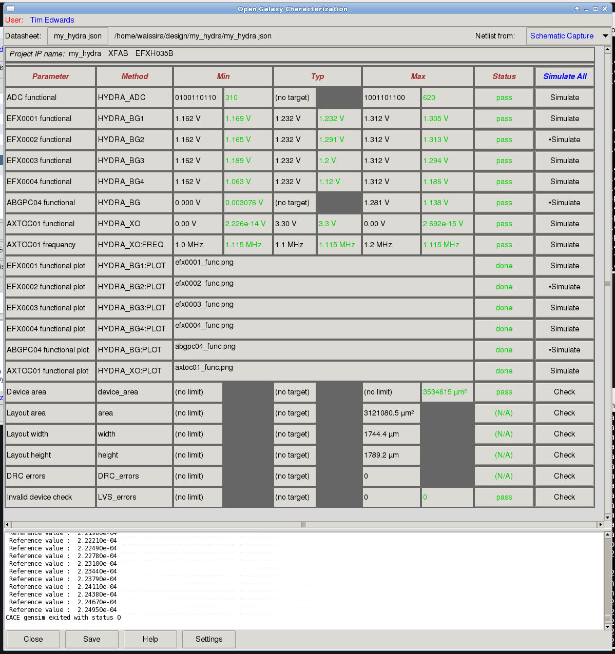
View of the characterization tool window for the my_hydra project after characterization.
Note the various functional tests and their results. The test of the ADC drives the ADC input at two different voltages (1.0V and 2.0V), runs the ADC conversion through the SPI interface, and records the result passed back by the ADC into the SPI registers. This is a sophisticated cosimulation that uses verilog to drive the SPI, acting like an off-chip piece of test equipment. The ADC’s physical implementation is a switched-capacitor circuit, and is difficult to simulate by itself, let alone within an entire chip’s circuitry. So the ADC has been replaced by a functionally equivalent XSPICE model. Even with the functional model, this is a long-running simulation and so has been reduced to measuring only two points, which appear in the Min and Max columns. The result is a 10-bit number, so (1.0V / 3.3V) * 1024 = 310, confirming the wiring of the ADC.
If you click on the button labeled “pass” on the ADC functional test row, you get a list view of the results.
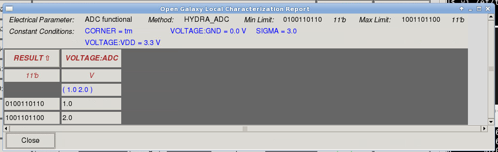
List view of the results for the ADC functional test.
The list view shows the conditions for each test, which in this case is the input voltage value into the ADC.
The functional results of the EFX* bandgaps are all very similar, because the circuits are all designed to the same specification. The results vary slightly in voltage due mainly to the settling time of the output vs. the short amount of time between measurements in the functional simulation. Again, click on the “pass” button to view the results. Those for the EFX0001 are shown below:
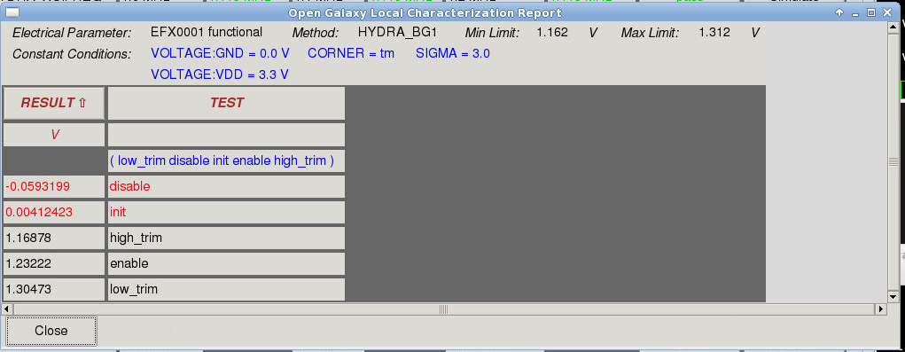
List view of results of the EFX0001 bandgap functional test.
Again, the table lists conditions for each test (most of which are constant over all measurements, and listed at top). The main variable “condition” is the name of the test itself, and shows that the output voltage is zero on chip power-on (because the default condition of each IP is to be disabled), has the expected voltage output at default, minimum, and maximum trim values, and returns to approximately zero volts when the IP block is disabled. All enabling, disabling, and trim setting is performed by communicating with the SPI through the verilog part of the testbench.
In addition to the pass/fail checks at top, the characterization tool provides additional tests in the form of plots, showing various signal values over time during the simulation. The plot below is the result for the EFX0003, which is simulated as a full-analog view, not a simplified functional view:
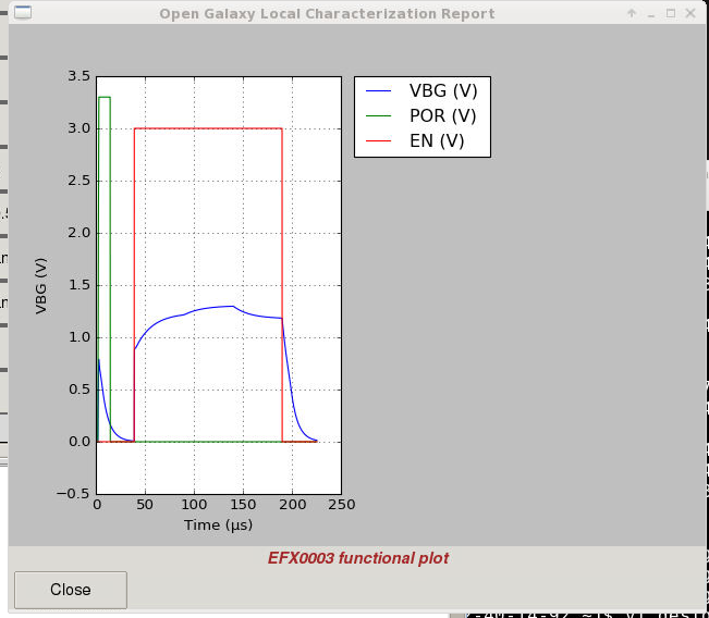
Functional test signal graph for the EFX0003 bandgap.
This plot includes the power-on-reset pulse from the power-on-reset circuit, the IP block enable signal that is generated from the SPI register, and the voltage output of the bandgap. While enabled, the bandgap is given two trim changes to maximum and minimum values.
The X-Fab bandgap IP is included on chip as a comparison to the challenge spec designs. However, it is a simpler bandgap that does not include a trim, so its functional test only exercises the enable and disable, as shown in the functional test plot result below:
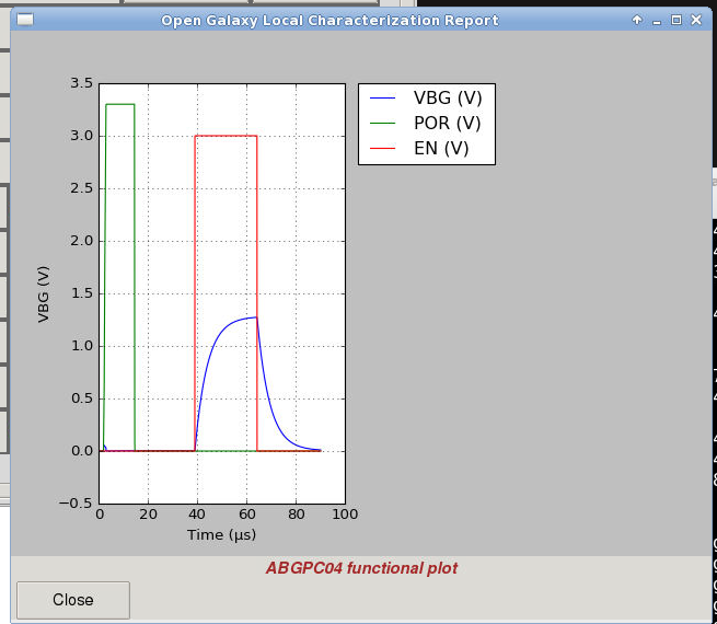
Functional test signal diagram for the ABGPC04 simple bandgap.
The hydra chip has a crystal oscillator built into the padframe. The oscillator design is another analog IP block from X-Fab, and nominally runs at 1MHz with the appropriate crystal applied. The crystal is modeled in SPICE according to the X-Fab documentation for the oscillator, and appears in the testbench netlist. In addition to the plot, there are two functional tests, one of which measures the peak-to-peak voltage output to check that the device gets properly enabled and disabled, and another test which measures the output frequency while the component is enabled. The plot reproduces the sequence of signals during the functional tests:
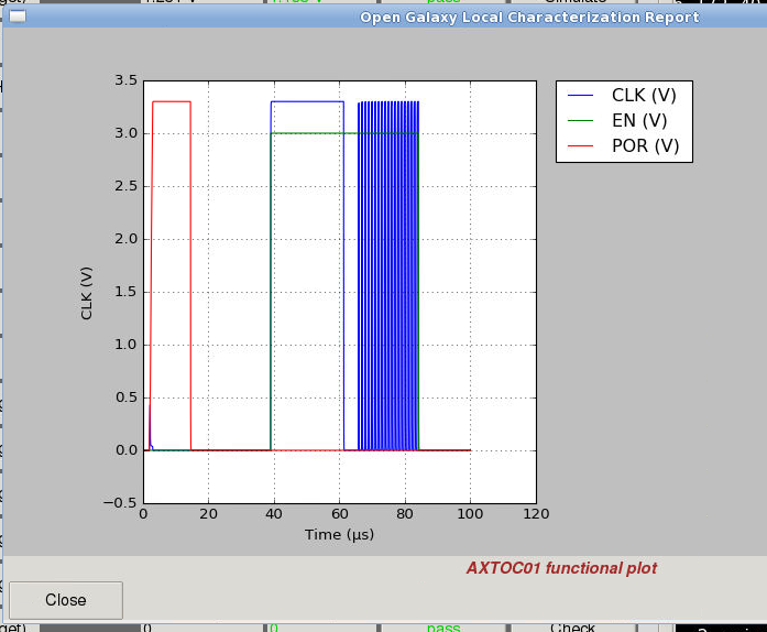
Functional test signal diagram for the AXTOC01 crystal oscillator.
The combination of functional simulation, LVS, and DRC is sufficient to ensure that first-time silicon will not fail due to incorrect wiring or incorrect understanding/interpretation of an IP block’s function, problems that can plague any chip design that does not include simulation of the entire device as it will be seen on the bench after manufacture and packaging. Of course it does not guarantee first-time silicon success, as it is up to the designer to provide a complete set of functional simulations to exercise all parts of the design. Other considerations such as the validity of each underlying IP block and the ERC (electrical rules check; e.g., check for ESD tolerance, metal migration, etc.) are intended to be correct-by-design if they are marked as “certified” IP in the Efabless catalog.
This article (part 3) has described full-chip functional testing from a prepared set of tests, using the Efabless characterization engine and a combination of simulators (ngspice using SPICE and XSPICE, and iverilog). The fourth part of this article gives additional detail about the testbench netlist and verilog and how to create or modify them for a new project, using the modified version of the “my_hydra” project that was described in Part 2.