![[object Object]](https://umsousercontent.com/lib_CUsguFEVafmoKCKW/ns6hm1s6vu8ctynd.png?w=334)
What is “Chiplicity”?
“Chiplicity” is the efabless.com methodology for building up complete chips ready for fabrication from component parts pulled from the Efabless IP catalog. This article (in four parts) describes the process of how to design and validate a complete integrated circuit chip on the Efabless platform.
The essential idea of “chiplicity” is that a complete integrated circuit chip should be built out of components which themselves are independently designed and characterized. The certifications found on designs in the Efabless IP catalog are indications that a design has passed critical checks and may be used as IP (intellectual property) within a larger framework such as a chip. To get certification, each design passes through an approval process, and in that process, is put into the IP catalog as a read-only project that can be downloaded as “Try Before Buy”. The view of this IP on the Open Galaxy design platform is either a symbol in a schematic or an abstract view in a layout, both showing pins and other essential information without revealing the detailed circuit contents. A chip-level design using these components can be validated without access to the protected IP contents. Simulations are done either using a process with elevated permissions, or else are done using validated abstract behavioral models of the IP blocks.
“Chiplicity” aims to make the design of complete systems easy to accomplish without high barriers to entry and steep learning curves.
The four parts of this article cover the following topics:
- How to clone a full-chip project from the existing “hydra” demonstration project in the Efabless IP catalog.
- How to run full-chip simulations to verify functional characterization of the “hydra” demonstration project.
- How to create your own chip based on the “hydra” architecture using the “hydra” project as a starting point.
- How to create and run new functional tests for your own chip-level project.
Example chip design: “my_hydra”
The first Hydra chip (hydra_v1p5) was a demonstration platform showing the capability of open-source tools on the Efabless platform to create working silicon. It was essentially a prototype of a prototype, and it proved its point that a complete, working chip can be designed and verified with an open-source toolchain. The second version of this chip (hydra_v2p0) is a test platform for the circuit design winners of the first Efabless design challenge (low power bandgap for the X-Fab XH035 process), but is also intended as an open-source demonstration platform for the toolchain that can be used as a starting point for other projects of similar scope. This second version of “hydra” was used to validate the basic premises of the “chiplicity” methodology. It was the first full-chip design to be done completely within the “chiplicity” framework (more or less, as the framework was being developed simultaneously), and all the IP block components of the chip have been placed in the Efabless IP catalog.
This article is largely a tutorial showing how to download the Hydra chip from the IP catalog, turning it into your own personal copy of the design which I’ll call, for the purposes of the article, “my_hydra”. You can then validate the existing design (see part 2) or reconfigure it for your own purposes (see parts 3 and 4).
Getting started
The first thing to do is to get your own personal copy of the Hydra chip. You need to understand the two main types of IP found in the catalog. Those designs that are open-source and may be copied from the catalog into a project in your Open Galaxy design workspace are marked with a button “Clone Hard IP”. Views of the design itself are unrestricted, although the design may contain restricted IP. When you Clone an IP, you will get complete schematics and layout for the design, and can simulate and verify the design. Those designs in the IP catalog that are closed-source and whose contents are protected are marked with a button “Try Hard IP”. Views of the design are restricted. When you Try an IP, you will get access to a symbol of the IP block for use in a schematic, and an abstract view of the IP block for use in a layout. You will have access to these views from the schematic and layout editors, but they will not appear among your projects in your workspace.
Designs which are open-source will (usually) also have a button for “Try Hard IP”. Just because an IP block is open-source does not necessarily mean that you will want to or need to edit it. Working with any block as an abstract view in both schematic and layout simplifies the process of building out and verifying the entire design. If you need a modified version of an open-source IP block, you can always include that in your design, but of course it will have to be validated locally.
A design like the Hydra chip is dependent on all of the IP blocks it contains. The Efabless web tools will make sure that when you Clone the Hydra IP, you also get all of the dependencies. Dependencies of a design are, by definition, protected views, even if the designs are open-source, because the protected views simplify the whole design process. As mentioned above, if you need to modify any dependent block, you can replace the protected view with a design from your workspace.
Go to the Efabless design catalog at this link: Design Catalog.
IP catalog initial view
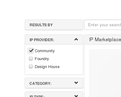
If no designs are showing in the window, then click on the “IP Provider” tab and select the checkbox next to “Community”.
IP catalog selecting content
Then press the search button (magnifying glass icon)

IP catalog initiating a search
to apply the filter and display the search results from the catalog.
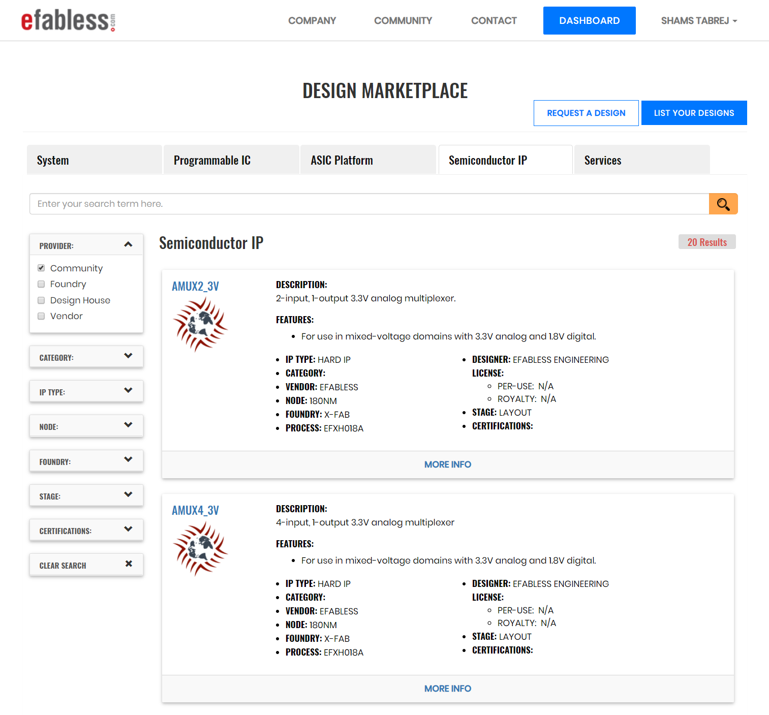
IP catalog showing community content
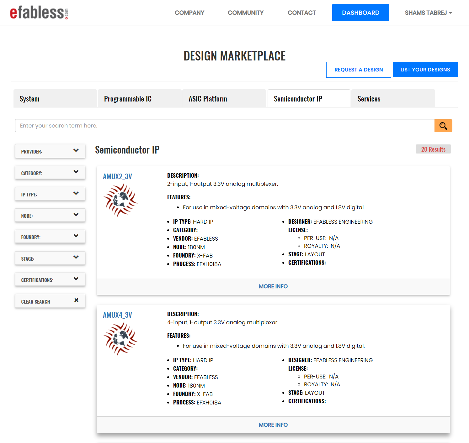
You can browse or search this page for the IP block called “Hydra v2p0”.
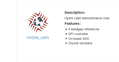
The entry for the hydra_v2p0 in the catalog
Click on the name or on the “More Info” button to view the details of the IP block. Go now to the detailed view of “Hydra_v2p0”.
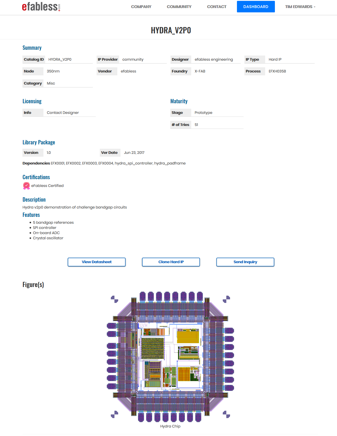
Detailed entry for hydra_v2p0 in the IP catalog
Cloning a project and MyLib staging
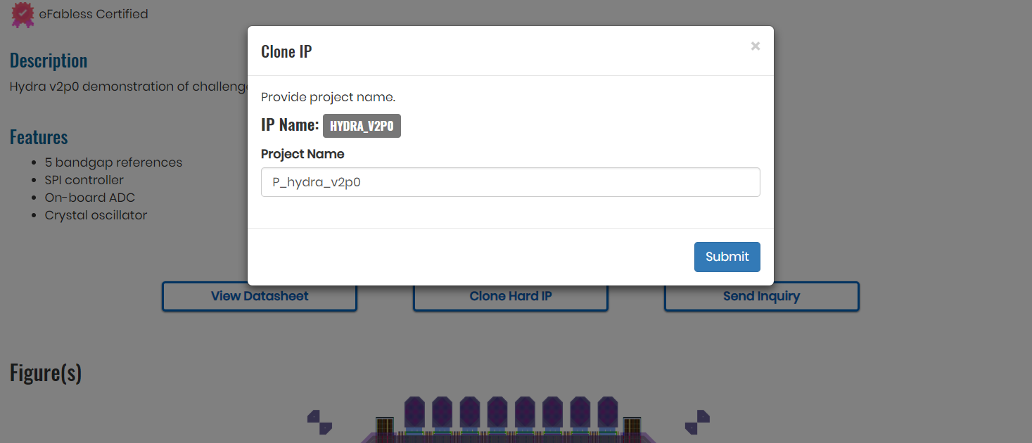
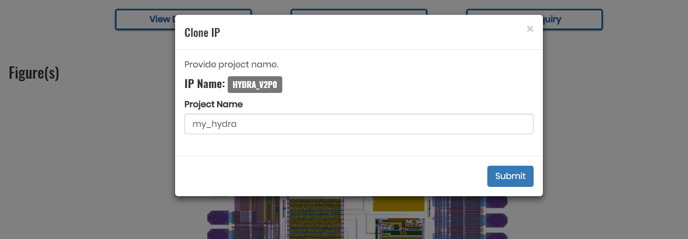
Clone the Hydra_v2p0 IP block by pressing the “Clone Hard IP” button. This is an open-source project and there are no fees or restrictions involved, so you are free to make as many copies as you like. However, the name “hydra_v2p0” is part of the Efabless IP catalog, and your cloned copy will be your own independent version of that design, so you will be asked to give it a new name. For the purpose of this article and tutorial, you can name it “my_hydra”.
As soon as the project has been selected for cloning, a message will appear at the top of the IP catalog page asking you to provide a new name for your personal version of the cloned project.
Selecting hydra_v2p0 for cloning
This is where you will provide the name “my_hydra” (or take the default suggestion, or use any name of your choosing).
Renaming hydra_v2p0 clone as a user project
Then click the “Submit” button. Now a message appears at the top of the catalog page saying “This item has been cloned to My Projects”.
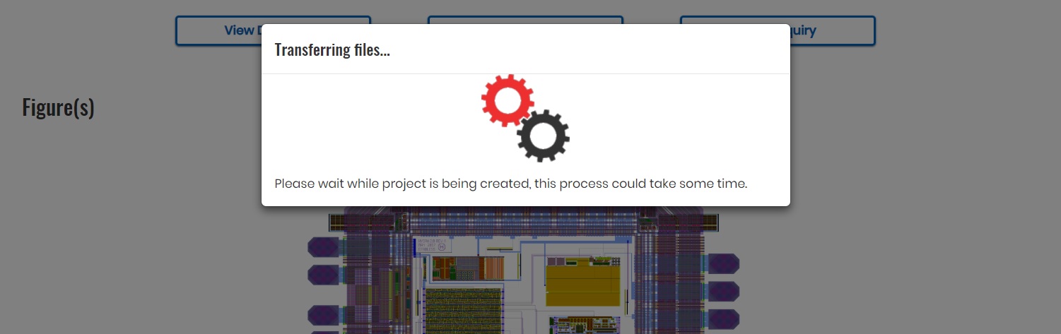
Transferring files to your hard Projects.Transferring files to your hard Projects.
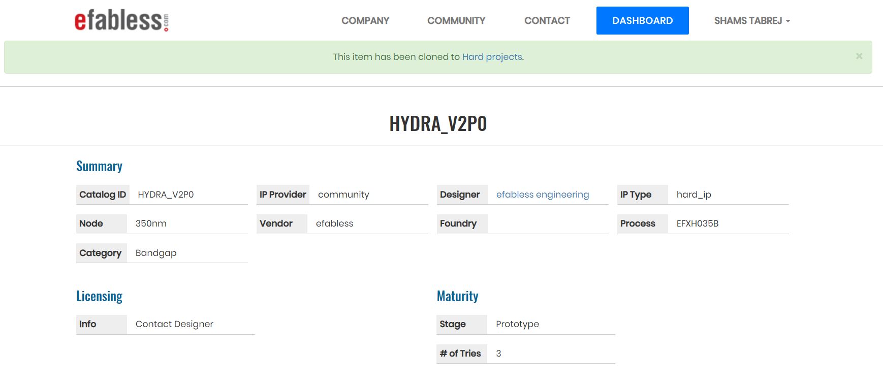
hydra_v2p0 project clone copied to Hard Projects
MY PROJECTS
hydra_v2p0 is now cloned to Hard projects, you can click the link in flash message and goto Hard Project Page or you can access that from dashboard. From my projects, this is already added to your project to OpenGalaxy. Here you should see the “my_hydra” project that you have just selected for cloning.
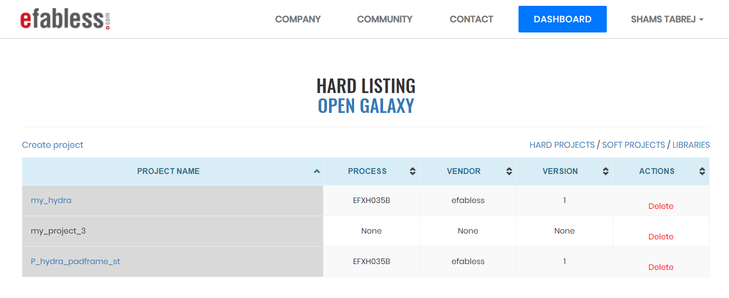
My Projects
The word “Libraries ” is a link that takes you directly to the “Library Listing”.
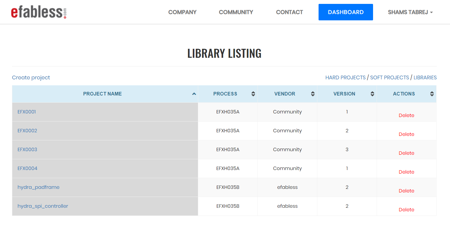
View of Libraries after cloning a project
Open Galaxy workspace
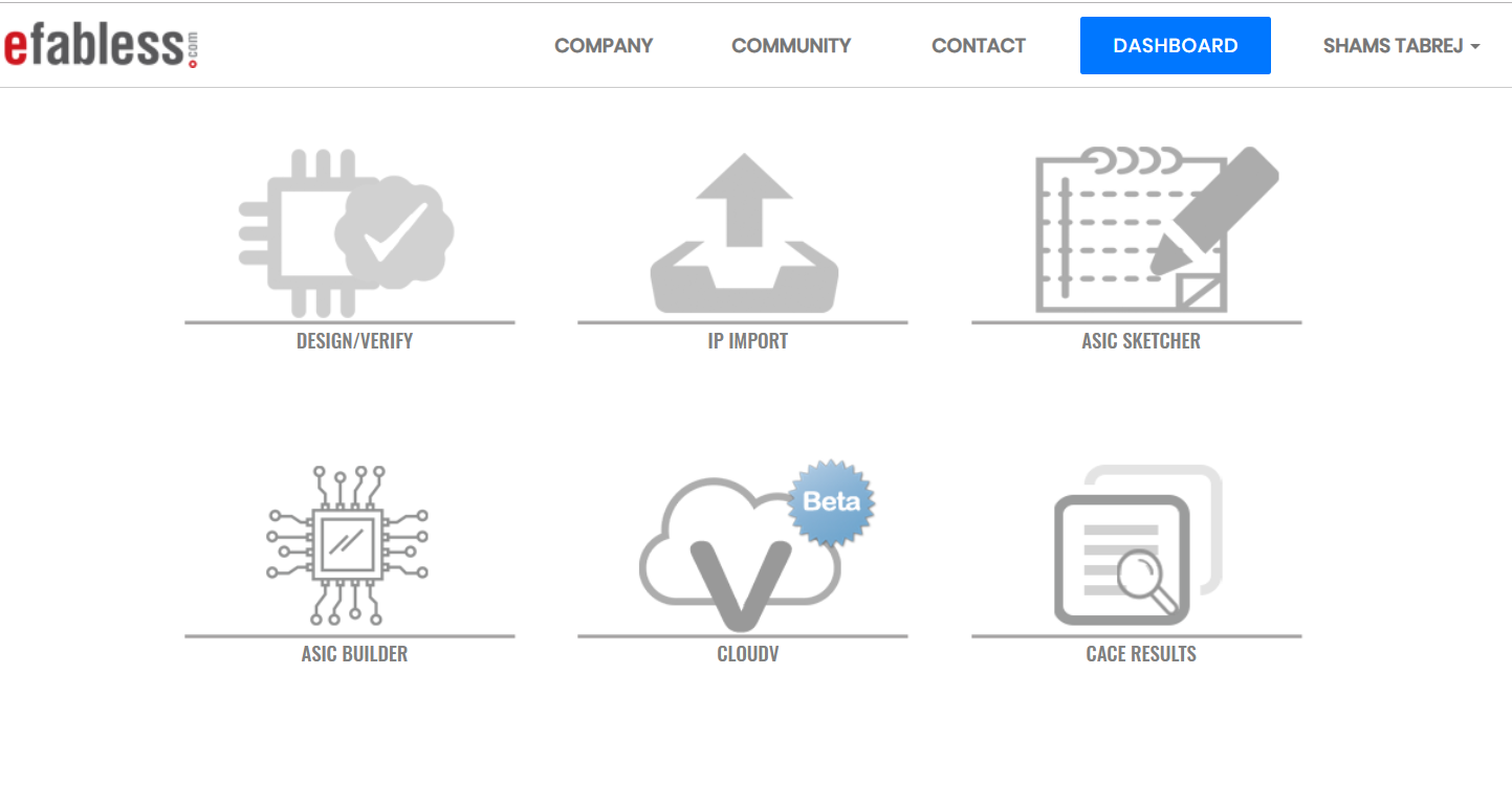
The second step is to access your workspace on Open Galaxy, which you do by going to the Efabless Dashboard,

Dashboard menu button on the Efabless web page
then selecting “Toolbox”,
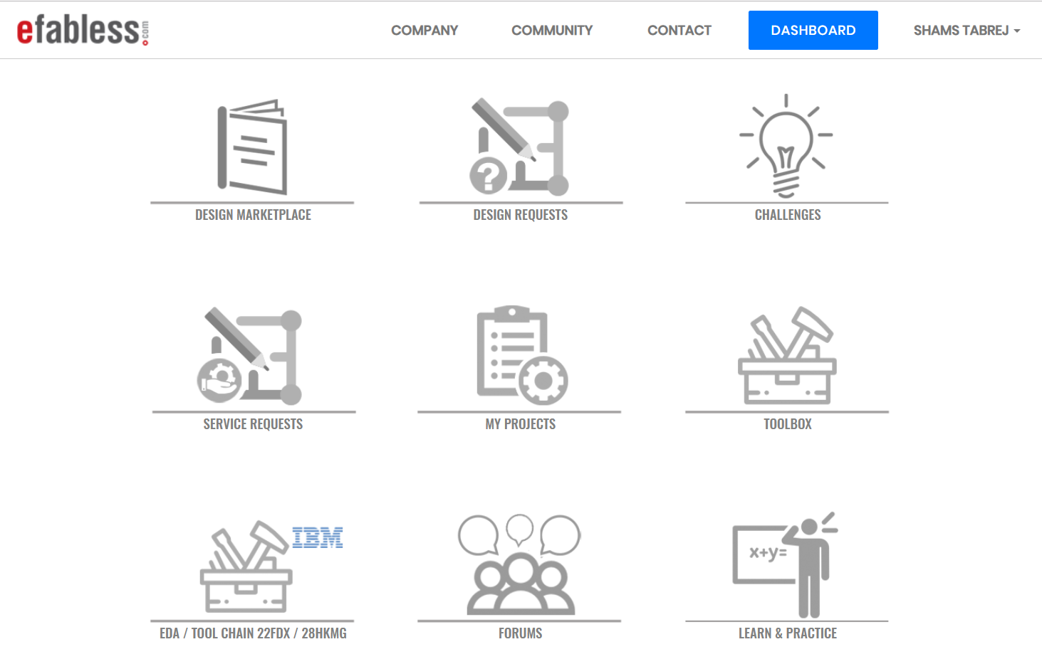
Website dashboard page
then “Design/Verify”.
Website toolbox page
This takes you to your Open Galaxy workspace where you can view and work on projects.
If you do not have a project manager running, then click on the Efabless icon in the lower left-hand corner of the window to launch it.
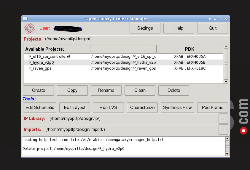
Open galaxy project manager
when you open the project manager you will see your project
Viewing the chip design
The chip design is easy to access from the Open Galaxy project manager. Just click on the line “my_hydra” in “Available Projects:”.
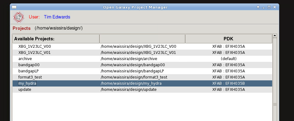
Selecting cloned project in project manager
Once selected, you can use any of the buttons “Edit Schematic”, “Edit Layout”, “Run LVS”, and “Characterize” to view, edit, and validate the project. Click on “Edit Schematic” now. This will start the Electric schematic editor. On the first launch, nothing will show in the window, but the tab “Components” on the left side of the window will have entries for “my_hydra”.
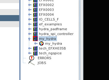
Electric view of project library
Expanding the “my_hydra” entry will show two items, a schematic and a symbol.
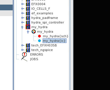
Project library expanded in Electric
Double-click on the symbol to see the symbolic view of the chip pinout.
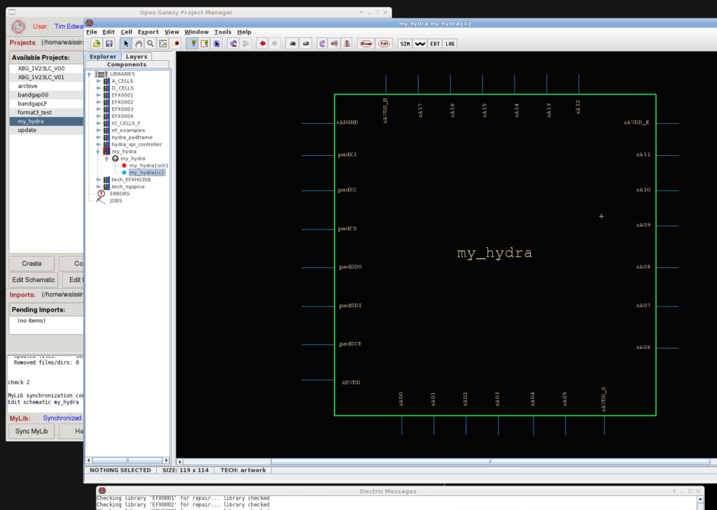
Electric symbol view of the hydra chip clone
Double-click on the schematic to see the complete chip schematic.
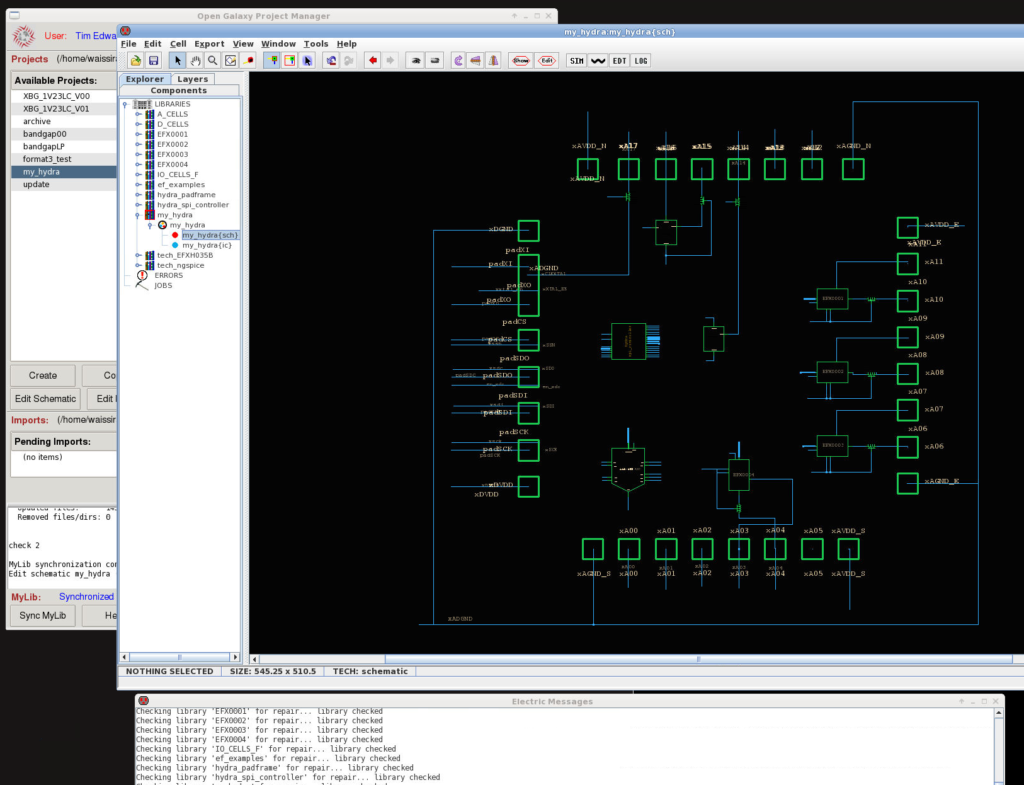
Electric schematic view of the hydra chip clone
My_hydra schematic
You will note that the schematic has more components than those that were downloaded from the IP catalog. That’s because some components belong to the fabrication process PDK (process design kit). They are part of the foundry IP and can be used without needing to download from the catalog. You will find all such foundry IP in the libraries at the top of the Components list (for my_hydra, that includes A_CELLS with analog IP such as the ADC and power-on reset (POR) circuit; D_CELLS for digital standard cells, and IO_CELLS for the pads in the padframe). You will also find libraries for each of the dependent IP blocks that were downloaded from the IP catalog as dependencies of the hydra_v2p0 design. You will note that as protected IP, each of these has a symbolic view but not a schematic view.
My_hydra layout
If you quit Electric and then click on “Edit Layout”, the layout editor Magic will start with a view of the full chip layout.
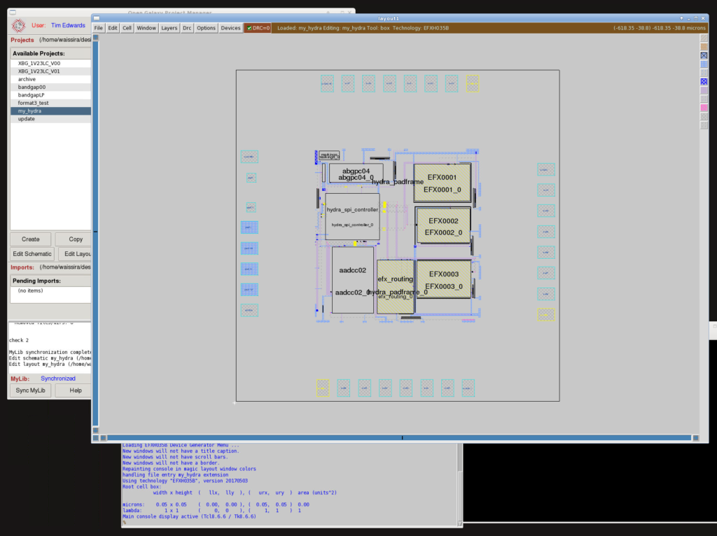
Magic unexpanded layout view of the hydra chip clone
You can select the whole chip in this view by putting the cursor over the background and typing “s” (or putting the cursor over the chip layout and typing “Control-i”), then typing “Shift-f” to expand to the full view.
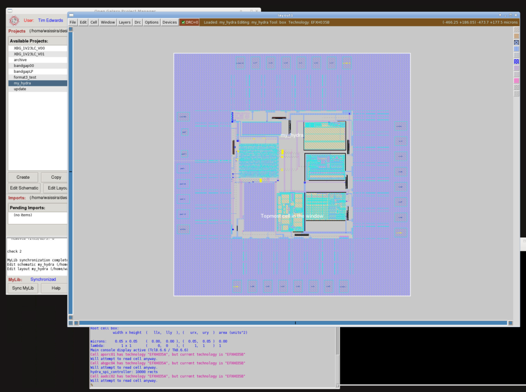
Magic expanded view of the hydra chip clone, with abstract views
The views you see of each of the IP blocks is an “abstract” view showing the name and position of each pin of the block layout, and showing where metal layers exist in the block that must be avoided by routing or any other metal structures placed in the top level of the chip layout. Not all the design hierarchy is restricted abstract views—you will notice resistors in the design that have been pulled from the PDK (in the “Devices” menu button on the layout editor) as well as some substrate contacts and antenna diodes.
The layout editor view is also the point of validation for layout design rule correctness. The title bar of the layout window will have a green-colored checkbox with “DRC = 0” showing that the design is DRC clean.
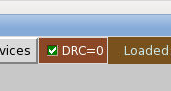
Magic DRC error indicator
The IP blocks for which you see only an abstract view are DRC clean by certification; if the design is layout-certified in the IP catalog, then it is guaranteed DRC clean. Obstruction layers in the abstract view plus prohibitions on overlapping IP blocks prevent DRC violations from being made on parts of the layout that cannot be directly viewed in the layout editor.
LVS verification
If you quit the layout editor and instead click on “Run LVS”, you will get the LVS (layout vs. schematic) manager window.
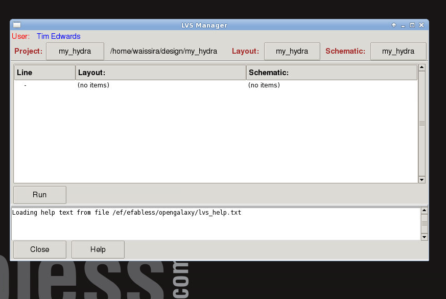
LVS manager window
Since all projects on the Efabless platform are set up with the same directory structure, LVS is as simple as pressing the “Run” button. Since the project has been verified before placing in the IP catalog, then the result of an LVS run should be clean if no edits have been made to either the schematic or layout views.
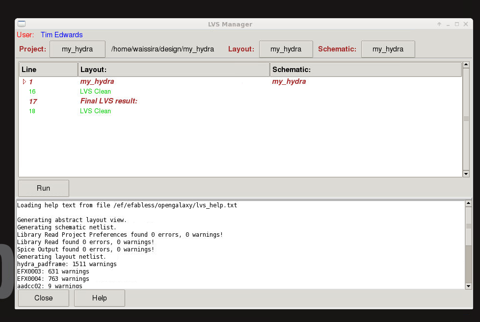
Hydra clone project showing LVS clean in LVS manager
If you expand the top line of the LVS results, you can see that as far as the LVS comparison tool is concerned, the chip has very little hierarchy, since most of the hierarchy is hidden within individual IP blocks, and those have all been abstracted into simple, flat views.
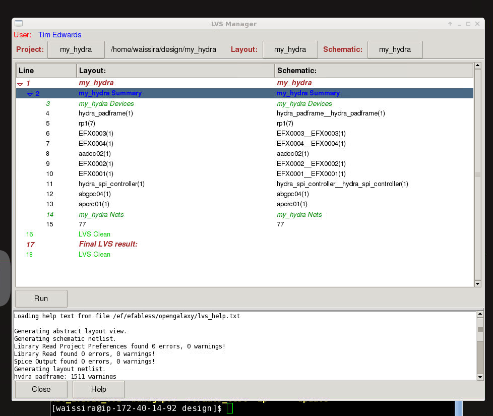
Summary view of hydra chip clone LVS
Characterization (see Part 2)
All official characterization is done through the characterization tool, accessed from the “Characterize” button on the project manager. Testbench simulations can be constructed and run from the Electric schematic editor, but the characterization tool runs automated checks to generate results to be viewed in the IP catalog, as well as officially validating the design. There are a number of functional tests for the “hydra_v2p0” project, which are covered in Part 2 of this article. There are also various physical parameters that can be checked, including the chip area, width, and height, and a device check to ensure that all devices are valid for the foundry process (check done on the schematic view), and DRC and LVS checks (done on the layout view). By default, the source netlist is set to be the netlist captured from the schematic view, and tests (where applicable) are run on this netlist.
Your Own Hydra (see Parts 3 and 4)
Now you have seen the complete hydra v2p0 project as it was designed. But the purpose of cloning a project is so that you can not only view the existing design, but also so that you can use the design as a starting point for your own project. Part 3 of this article outlines how to modify a cloned project like the Hydra v2p0 chip to your own specifications, and Part 4 shows how to design and run full-chip functional simulations on your own chip design.