![[object Object]](https://umsousercontent.com/lib_CUsguFEVafmoKCKW/ns6hm1s6vu8ctynd.png?w=334)
Did you hear about an upcoming IC circuit design challenge from Efabless? Well, this article will help you navigate through the application process for a design challenge. First, go to the main site of efabless.com

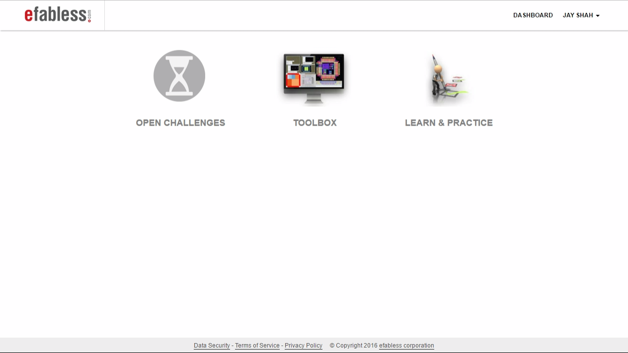
The dashboard is your launchpad to various features of Efabless’ offering. Feel free to explore other aspects of Dashboard. For now, we will go to OPEN CHALLENGES
After reading through challenge announcement, if your curiosity levels have spiked, you can further click on the View Detailed Specifications. This page takes you a step closer towards the current challenge in hand.
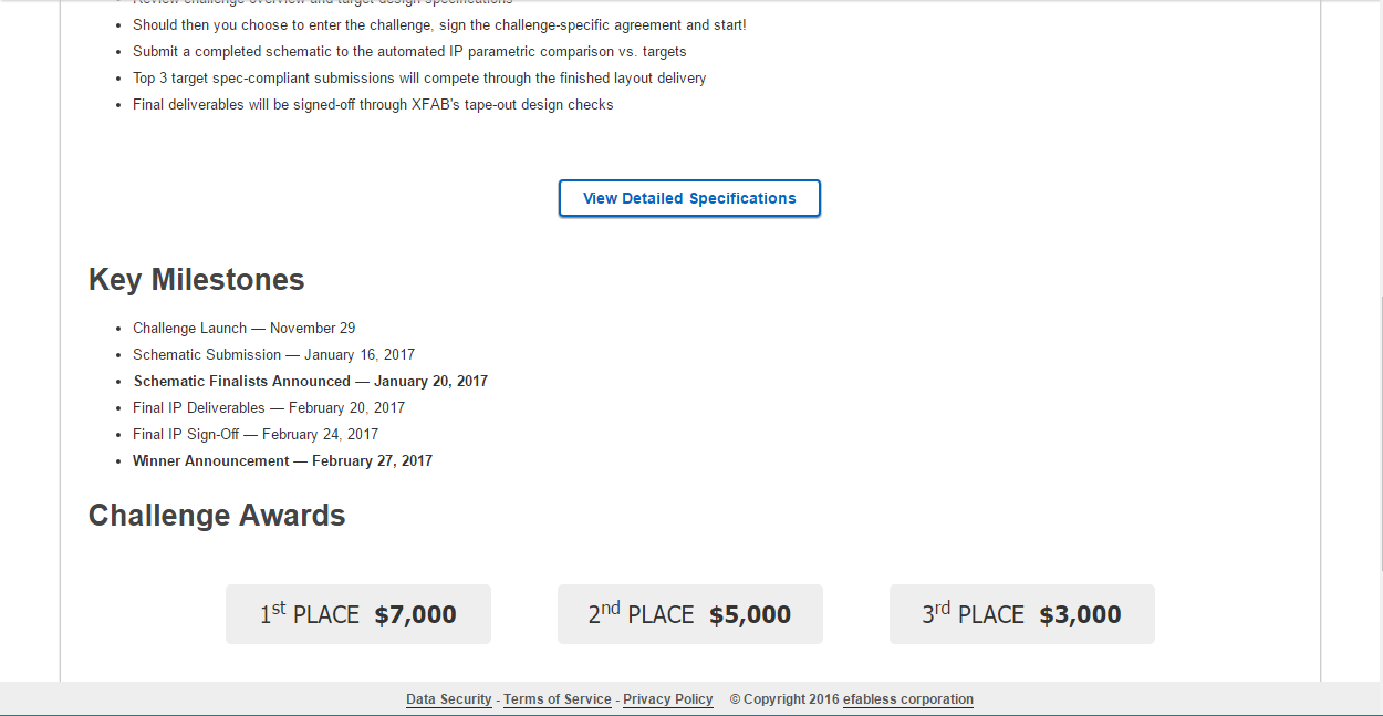
The detailed specification page lists the target specifications for the given challenge, as well as information about the deliverable design briefly. If you have any further questions about challenge specification page, you can email us at helpdesk@efabless.com
If your excitement is resonating with the design challenge ahead of you, click on Accept button on the bottom of this page to get onto the last step of being part of this design challenge.
This will bring you to the final step of challenge accepting the challenge – the design challenge terms. We encourage you to read this thoroughly before accepting the challenge. With everything in agreement, upon clicking on the confirm button, you will be greeted with the following page:
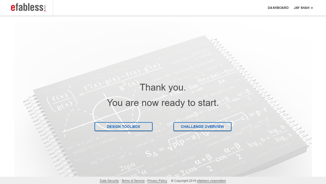
You can choose to review the challenge target specifications or proceed ahead to use your virtual design space Open Galaxy

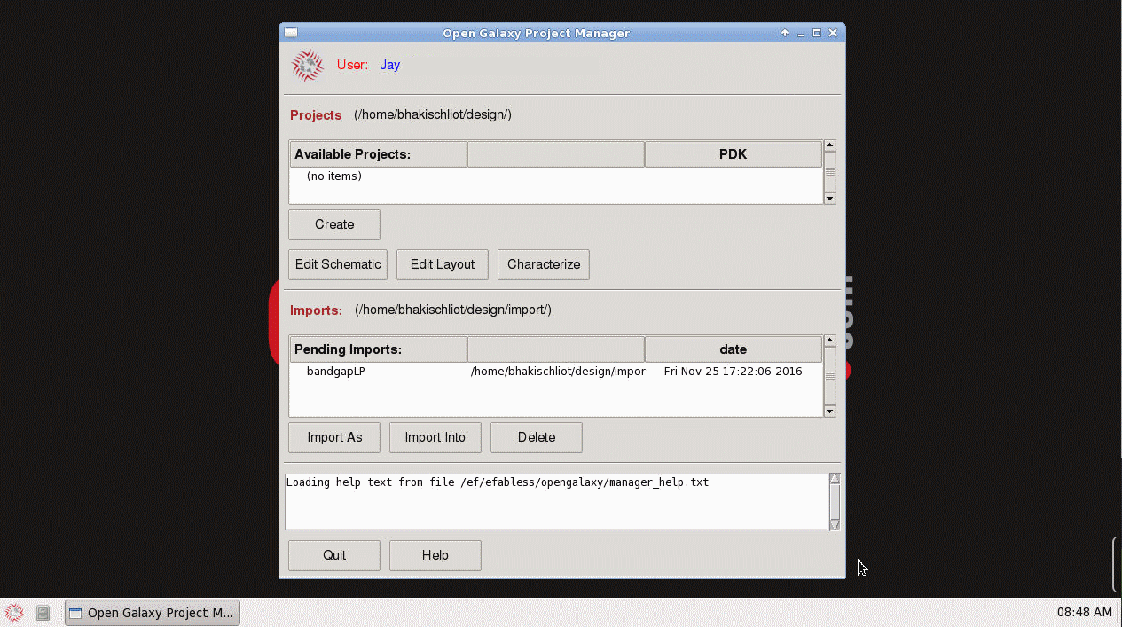
Let’s start with project manager. The project manager is a launchpad to get across various tools throughout your design project lifecycle.
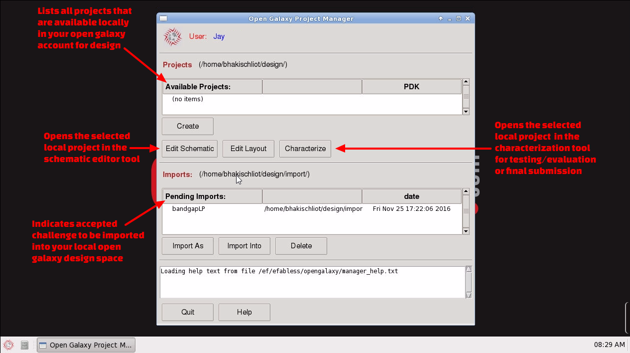
We will now import challenge project files into our design space.
That’s it. Now you can open schematic editor to get started with schematic design process of the challenge.